Eight Keys, One Lock: How an Advanced Chip Gets Built
No country on Earth can build an advanced chip alone. A tour through the eight chokepoints of the most concentrated supply chain ever assembled — and the dependency-mapping lessons that apply to any company, not just chipmakers.

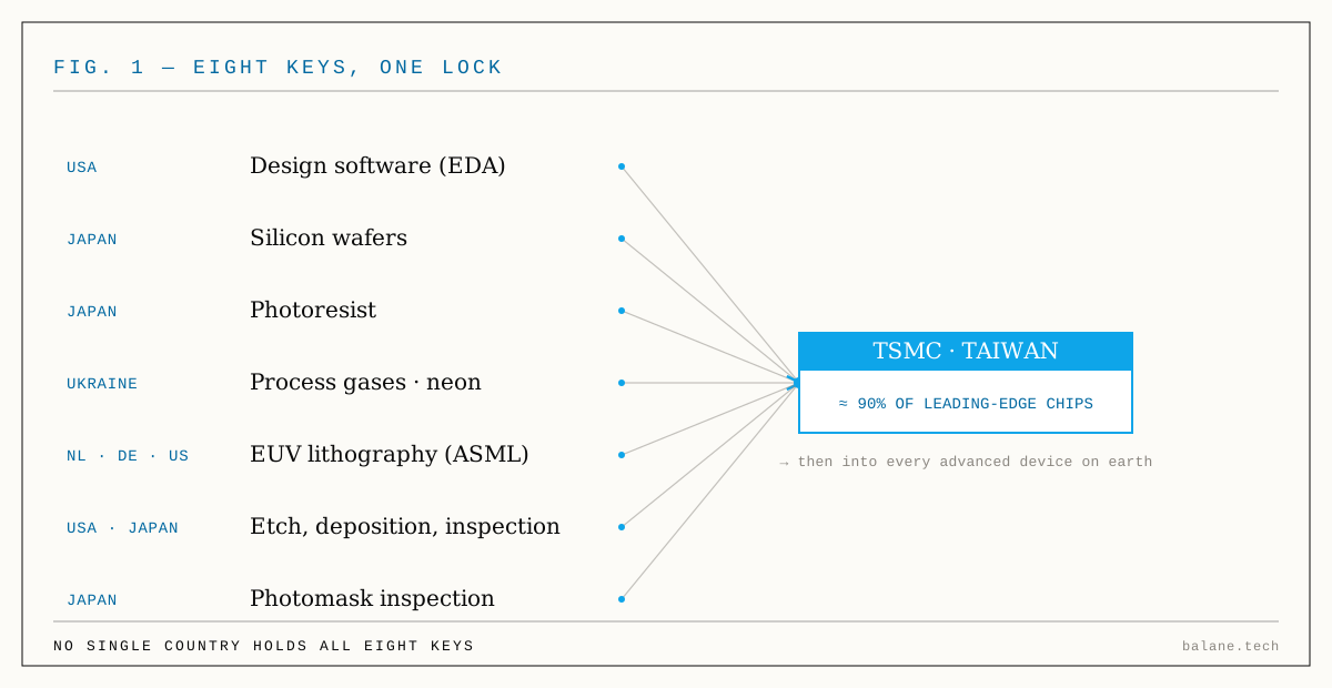
Eight Keys, One Lock: How an Advanced Chip Gets Built — and What Its Supply Chain Teaches Every Business
No country on Earth can build an advanced chip alone. Not China, with all its capital and manufacturing muscle. Not the United States, which designs most of them. Not even Taiwan, which fabricates almost all of them. The most consequential object of the modern economy — the few square millimetres of patterned silicon behind every phone, car, and AI model — is assembled from a chain of dependencies so specialised that no single nation controls even half of it.
In an earlier piece on concentration risk we argued that concentration is a structural risk regardless of who holds the concentrated position — and we named advanced semiconductors as the single sharpest chokepoint in the whole software stack. This article zooms into that one layer. The zoom is worth it, because the chip supply chain is the clearest working model of dependency risk ever built. And its most useful lessons have almost nothing to do with chips.
The lock and its eight keys
Think of a finished leading-edge chip as a lock that opens only when eight separate keys are turned in sequence. Each key is a step in the process. What makes the industry extraordinary is not that the steps are hard — it's that almost every one of them has narrowed, over decades, to a single company or a single country. Lose any one, and the whole line stops.
Let's turn the keys one at a time — not to catalogue an industry, but to watch a pattern repeat.
Before any silicon is touched: the design
A modern chip carries tens of billions of transistors. No human draws that by hand; it is designed entirely in software called EDA — electronic design automation. And that software is a near-textbook oligopoly. Three firms hold roughly three-quarters of the market between them: Synopsys (~31%), Cadence (~30%), and Siemens EDA (~13%) — the last one American-built (it grew out of Oregon's Mentor Graphics) but German-owned. Every Apple chip, every Nvidia GPU, every custom accelerator is designed in one of these three toolchains.
Why only three, in a world drowning in software companies? Because EDA is not ordinary software. It took forty years to accumulate, and its hardest job is to prove — mathematically, before anything is manufactured — that billions of transistors will behave. The cost of getting it wrong is brutal: a mistake caught only after the design goes to the factory means a "re-spin," and at the leading edge a re-spin runs $50–100 million and six to twelve months lost. When the penalty for error is that steep, buyers do not shop around. They stay with the toolchain they trust, and the incumbents compound.
The materials almost no one can make
The wafer is a polished disc of silicon so pure it is measured in "nines" — only a handful of contaminant atoms per billion. Misplace a single one in the crystal, and the defect propagates through every layer built on top. Two Japanese firms, Shin‑Etsu Chemical and SUMCO, are the largest makers of these advanced wafers, and Japan's producers together account for the majority of global supply. The reason is unglamorous and hard to copy: decades of precision-materials culture, chemical and equipment suppliers clustered in the same region, and — the real selling point — lot-to-lot consistency sustained over thirty years.
Then comes the ink. Photoresist is the light-sensitive coating that lets a lithography machine transfer a pattern onto the wafer; without it, the most advanced machine on Earth prints nothing. And here the concentration is near-absolute. Japan produces roughly 90% of the world's photoresist, and for the advanced resists used at the leading edge it is effectively the only supplier — the key names are JSR, Tokyo Ohka Kogyo, and Shin‑Etsu. The same country holds around 90% of fluorinated polyimide and 70% of the specialised etching gas (hydrogen fluoride) the fabs depend on.
That is not a neutral fact — it is a lever, and it has been pulled.
In July 2019, Japan quietly moved exactly three materials — advanced photoresist, hydrogen fluoride, and fluorinated polyimide — from routine export to case‑by‑case licensing for South Korea. It was not a full ban, but it did not need to be. Korea was importing 92% of its photoresist and 94% of its fluorinated polyimide from Japan, and the move landed directly on Samsung and SK Hynix — two companies that between them make around two-thirds of the world's memory chips. A change in one country's paperwork became an existential question for another country's flagship industry, overnight.
The fourth material is stranger still. The lasers inside lithography machines need neon gas of extreme purity — and in 2022, roughly half the world's neon came from Ukraine, a legacy of the Soviet-era steel industry, whose vast air-separation plants captured neon as a byproduct. Two firms, Ingas and Cryoin, supplied much of the world's semiconductor-grade neon. (A common myth conflates two shocks: the dramatic ~70% supply figure and a ~600% price spike belong to the 2014 Crimea episode, not the 2022 invasion — a useful reminder that supply-chain scares get mythologised, and that numbers deserve checking before they get repeated.) The deeper point holds either way: a chokepoint you have never heard of, in an industry that looks nothing like electronics, can sit two steps upstream of every chip you own.
The one machine — itself a small United Nations
To print the smallest features on a leading-edge chip you need extreme-ultraviolet (EUV) lithography, and there is exactly one company on Earth that makes an EUV machine: ASML, in Veldhoven, the Netherlands. Not a dominant share — the whole market. It builds around fifty of these machines a year, at roughly $380 million each (the newest generation approaches $400 million), on gross margins that only a genuine monopoly commands.
Why the Netherlands, and not Germany or Switzerland? The honest answer is not geography but history: ASML was spun out of Philips, which had been doing precision optics and photolithography for its own consumer electronics since the 1960s. No neighbour had an equivalent starting point, and thirty years of supplier relationships cannot be conjured on demand.
And even this "one machine" is not really one country's. ASML integrates far more than it manufactures; its scanners contain over 100,000 components from a network of thousands of suppliers. Two are irreplaceable. The mirrors — the most precise objects made at industrial scale, polished to roughly 50-picometre accuracy — come from Germany's Carl Zeiss SMT, effectively the sole source of EUV optics, built on decades of research and thousands of patents. The light source comes from Cymer, a US company ASML acquired in 2013. So the single most critical tool in the entire chain is itself Dutch, German, and American at once — a supply chain nested inside a supply chain.
That nested dependency is also the reason China cannot simply buy its way in. Because the light source is US-origin technology, Washington can reach ASML's Dutch-made machines through the Foreign Direct Product Rule — and a coordinated US–Dutch–Japanese export regime has, since 2019, kept advanced EUV out of China entirely.
- Jul 2019Japan → South KoreaThree materials shifted to case-by-case licensing, squeezing Samsung and SK Hynix. A dispute about history, fought with supply chains.
- 2019 onwardThe EUV machine that never shippedUnder US pressure, the Dutch government did not renew ASML's licence to sell an EUV system to China's SMIC. It was never delivered.
- 2020The US extends its reachWashington expands the Foreign Direct Product Rule so that any chip made with US technology falls under its controls.
- Jan 2023 onwardA three-country blocThe US, Netherlands and Japan align their controls; the Netherlands restricts advanced DUV tools, Japan restricts 23 categories of equipment.
Where it all converges: Taiwan
The remaining keys — the tools that etch, deposit and inspect each layer, and the stencils ("photomasks") the patterns are printed from — sit mostly with a short list of American and Japanese firms: Applied Materials, Lam Research, KLA, and Tokyo Electron. One deserves a special mention for how small-but-total a monopoly can be: the tools that inspect the photomasks themselves for defects come, almost exclusively, from a single Japanese company, Lasertec. Tiny in revenue, absolute in function. Skip that one inspection and a single undetected flaw on a mask reproduces onto every chip printed from it.
All eight keys converge in one place. For nearly forty years, the companies that design the world's chips — Apple, Nvidia, and the rest — have not built them. They send the designs to a foundry, and the foundry that matters is TSMC in Taiwan. When Morris Chang founded it in 1987, he made a bet that most chip companies would rather not own factories at all. He was right, and the bet compounded into something close to a natural law of the industry: today roughly 90% of the world's leading-edge chips are made on one island. The US Treasury Secretary has called Taiwan the world's single biggest point of failure — and analysts estimate a conflict there would cut off about 90% of the most advanced semiconductors overnight.
Why the map matters more than the machines
Here is where chips stop being the subject and start being the case study. Strip away the physics and three transferable truths remain — each one relevant to a company that has never been near a cleanroom.
Concentration is a property of design, not a forecast of failure. A supply chain that narrows to a single source or single location that one shock can disable is, by definition, a single point of failure — analysts call it focused risk. It may run flawlessly for years. Its vulnerability isn't bad luck waiting to happen; it's a structural feature you either chose on purpose or backed into by accident. Taiwan is the textbook example precisely because it works so well, right up until it doesn't.
Availability can be political. The June 2026 export directive that briefly switched off two AI models for every customer, the 2019 materials squeeze on Korea, the EUV machine that never shipped to China — none of these was an outage, an insolvency, or a price hike, the three risks every vendor assessment screens for. Each was a decision taken in a jurisdiction the dependent party does not vote in. A critical function with no second source is not an advantage; it is an exposed flank.
The real moat is rarely the money. A leading-edge fab costs $15–20 billion or more — you could build three World Trade Centers for less. But capital is the easy part of the barrier. What competitors cannot buy is what TSMC accumulated across four decades: the data from millions of chips, every defect and adjusted parameter, the tacit knowledge of an ecosystem of suppliers clustered within an hour's drive that can respond to a production problem the same afternoon. Intel has the largest R&D budget in the industry and is still catching up. The moat is institutional knowledge, and institutional knowledge does not accept wire transfers.
Note where the useful target sits: not at self-sufficiency, which is neither achievable nor desirable, but at optionality — the ability to switch without stopping. That target is reachable. It is a question of architecture, not of building a national champion for every input.
Two strategic choices worth stealing
The chip industry also offers two positioning lessons that any company can lift, because they answer a question every business faces: given a value chain, where is the defensible place to stand?
Japan answered it by owning the inputs rather than the visible product. It had a dominant chip-manufacturing industry in the 1980s and lost it — the economics of fabrication grew too capital-hungry. Rather than fight that losing battle, Japan retreated upstream and made itself indispensable in materials and equipment instead: the photoresist, the wafers, the specialised gases and tools that every fab on Earth needs, whoever wins the fabrication race. It is a quieter position than owning the famous end-product — and far more defensible.
ASML answered it by staying a neutral enabler rather than competing with its customers. It could, in theory, use its monopoly to start making chips itself. It doesn't — because the moment it did, it would become a rival to TSMC, Samsung, and Intel, and those customers would race to fund an alternative supplier. Its monopoly is more valuable precisely because it stays in its lane. Being the indispensable supplier to everyone beats being one more competitor to someone.
What this means for your business
You do not run a fab. But you run on a chain of dependencies, and most of its chokepoints are invisible until one of them fails. The chip industry's lesson is a discipline, and it is unglamorous — which is exactly why it works.
- Map the chain, then look for the single keys. For every critical function — a supplier, a platform, an integration, a person — ask what happens if it disappears for a quarter. The exposures that matter are rarely the ones on the risk register; they are the ones so reliable that nobody thought to list them.
- Make a second door a requirement, not a hope. For anything critical, the question is not only "how good is it?" but "how do I get out?" Data export, open formats, documented interfaces, and a swappable design belong in the contract, not the wish list.
- Find the person who is a single point of failure — and it is usually a person. In most mid-sized companies, the real chokepoint is not a foreign supplier; it is the one colleague who alone understands the pricing, the dispatch, the legacy system. That is your TSMC. Get the knowledge out of the single head and into a system before you are forced to.
- Decide where you want to stand. Not every advantage lives in the product you sell. Sometimes the defensible move is to own an input others depend on, or to become the neutral partner nobody can afford to replace.
Our position
At balane we build software for mid-sized companies — we advise, develop, and automate, and we look at every project through three lenses at once: business, psychology, and technology. The chip supply chain is, unexpectedly, a near-perfect illustration of why those three belong together.
The business lens is the map: where the concentration sits, which dependency is a genuine single point of failure, and where the defensible position actually is — sometimes an input, not the end-product. The technology lens is the second door: architecture built for portability and swappable building blocks, so a forced change is a configuration and not a crisis. And the psychology lens is the one people forget — because the deepest moat in the whole industry, TSMC's four decades of accumulated know-how, is tacit knowledge living inside an organisation. The same is true in miniature inside your company: the most fragile dependency is usually the knowledge that lives in one person's head, and getting it into a shared system is as much about trust and habit as it is about code.
None of this is a counsel of paranoia. It is the opposite — the calm recognition that resilience is designed in, one concrete decision at a time. That is where we work.

